The quest for materials that can enhance the performance of electronics beyond the limitations of silicon-based transistors has led researchers to explore the potential of two-dimensional (2D) semiconductors. These atomically thin materials have shown promising properties, such as high carrier mobilities and thin layers that could improve the performance of transistors. However, despite their advantages, 2D semiconductors face challenges due to high contact resistances linked to Fermi-level-pinning effects.
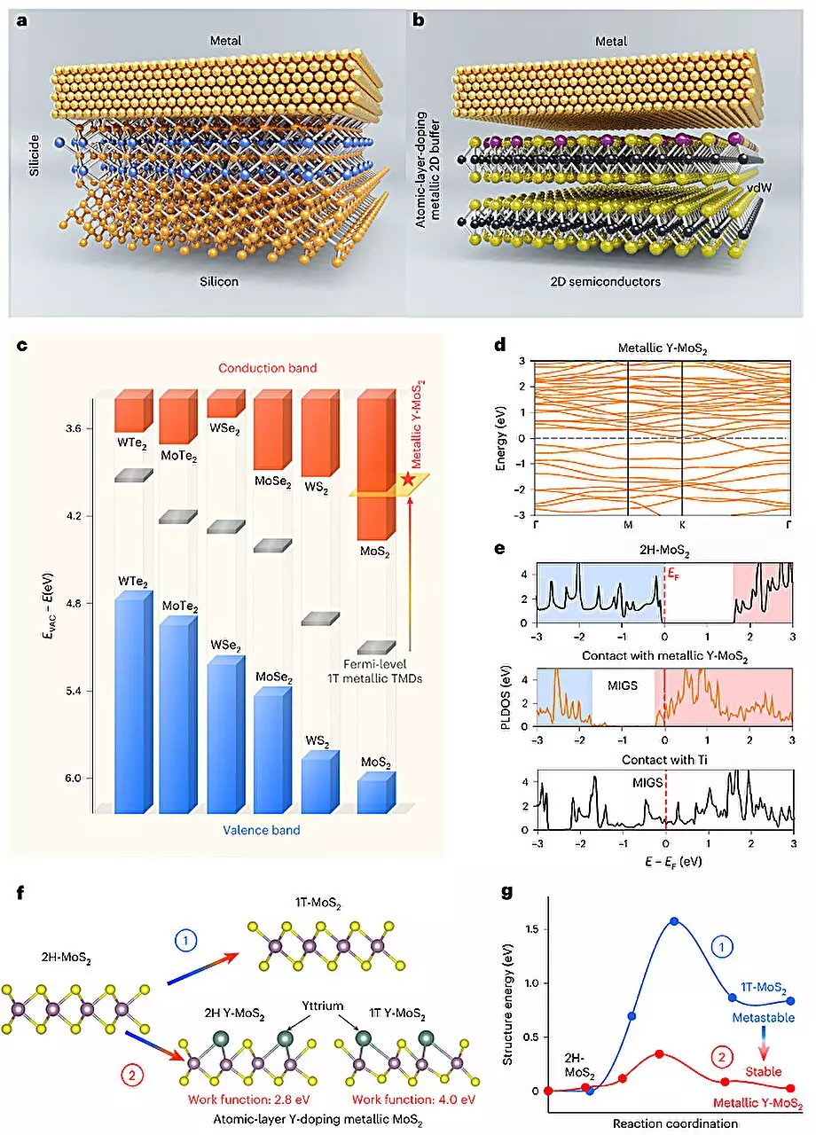
Recently, researchers from Peking University and the Chinese Academy of Sciences introduced a novel yttrium-doping strategy to address the key limitation of 2D semiconductors. By doping semiconducting molybdenum disulfide (MoS2) with yttrium, the researchers were able to convert it into a metallic form. This conversion improved band alignment and facilitated the fabrication of ohmic contacts for 2D transistors. The strategy involved placing a semi-metal layer between a metal electrode and the semiconductor, enhancing carrier injection efficiency.
To achieve yttrium doping in MoS2, the researchers developed the plasma-deposition-annealing (PDA) method. This technique involved treating patterned contact areas with low-power plasma to create active sites, followed by the deposition of a Y/Ti/Au stacked metal with Y as a solid-state doping source. The Y atoms diffused into the active sites and were activated through high-temperature annealing in an inert gas environment. The PDA doping process demonstrated great thermal stability, making it compatible with advanced-node wafer-scale integration.
Through their research, the team introduced the concept of a “rare earth element yttrium doping-induced 2D phase transition.” This phase transition led to the metallization of MoS2, enabling the development of ultra-short MoS2-based channel ballistic transistors with improved performance as ohmic contacts. The breakthrough in achieving a doping depth pushed to the atomic layer limit of 0.5 nanometers could pave the way for the development of new sub-1 nanometer node chips with enhanced performance and lower power consumption.
Looking ahead, the researchers aim to continue exploring the potential of yttrium-doping in developing p-type ohmic contacts suitable for 2D semiconductors. These advancements could contribute to the creation of innovative electronic devices with superior performance metrics while consuming minimal power. The integration of yttrium-doped 2D semiconductors in electronic applications holds the promise of revolutionizing the field of electronics and paving the way for more efficient and powerful devices.
The introduction of yttrium-doping strategies represents a significant leap forward in the development of 2D semiconductors. By overcoming the limitations associated with traditional materials, researchers are opening new doors for the advancement of electronic technologies. With further research and refinement, these novel approaches could usher in a new era of high-performance electronic devices that push the boundaries of what is currently possible.
Leave a Reply