The field of quantum sensing has taken a significant leap forward with the development of a new 2D quantum sensing chip using hexagonal boron nitride (hBN). This groundbreaking technology, developed by researchers at TMOS and RMIT University, promises to revolutionize the way we detect temperature anomalies and magnetic fields in any direction. The paper, published in Nature Communications, unveils a sensor that is thinner and more versatile than current quantum technology for magnetometry.
Traditionally, quantum sensing chips have been made from diamond due to its robust platform. However, diamond-based sensors have limitations when it comes to detecting magnetic fields. These sensors can only detect magnetic fields when aligned in the direction of the field, leading to blind spots if unaligned. This necessitates the use of multiple sensors at varying degrees of alignment, making operation more complex and limiting versatility in different applications. Moreover, the rigid and three-dimensional nature of diamond sensors restricts their ability to get close to samples that are not perfectly smooth.
In response to these limitations, researchers at TMOS and RMIT University are spearheading a new quantum sensing platform using hBN. Unlike diamond, hBN crystals are flexible and made up of atomically thick sheets, allowing sensing chips to conform to the shape of the sample being studied. This flexibility enables the sensors to get much closer to the sample, offering a significant advantage over diamond-based sensors.
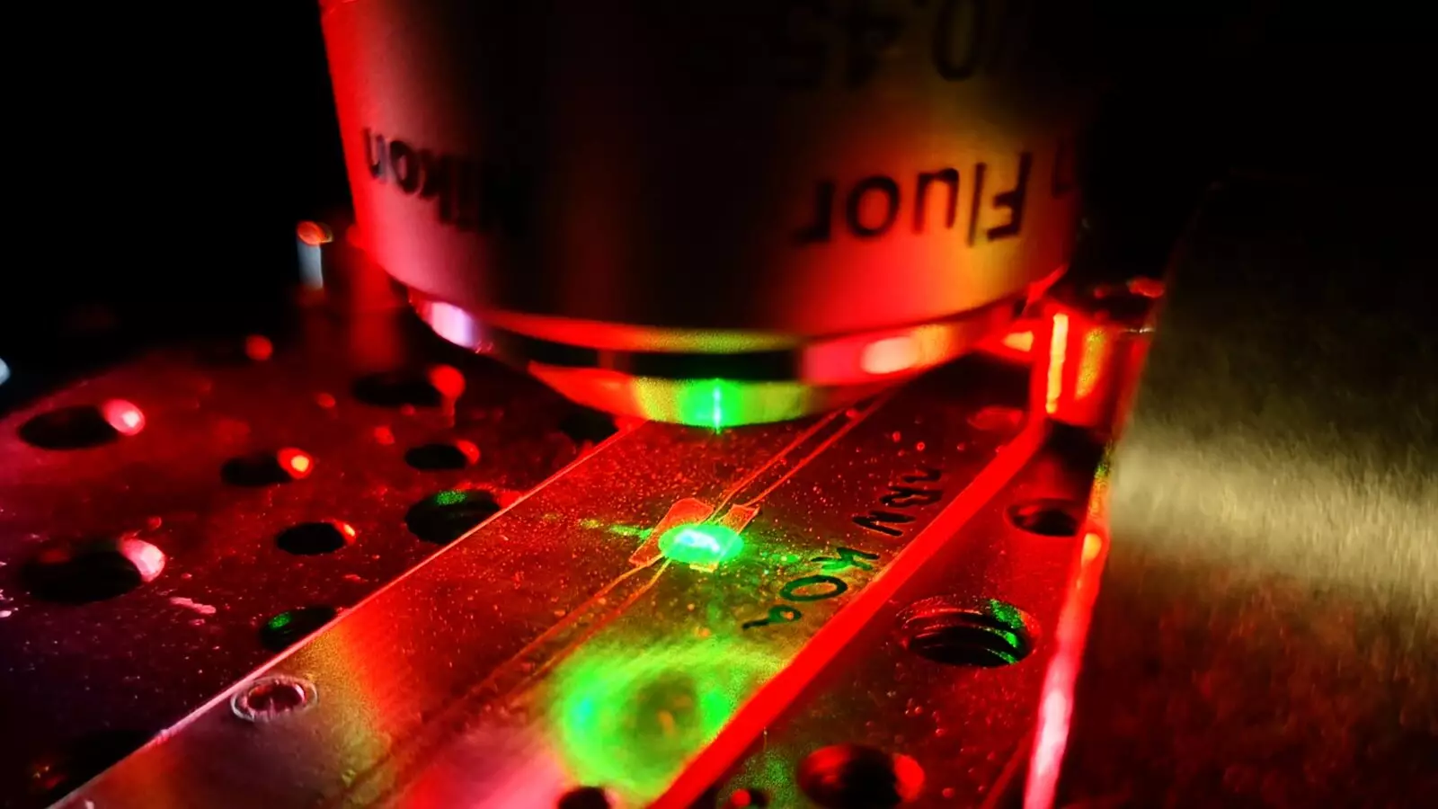
One of the key discoveries in this research is a recently identified carbon-based defect in hBN that can detect magnetic fields in any direction. This defect, with an unidentified atomic structure, behaves as a spin half system, enabling the sensor to detect magnetic fields with unparalleled accuracy. By running a Rabi measurement experiment and comparing the results with a well-understood boron vacancy defect in hBN, the researchers were able to characterize the new carbon-based defect and demonstrate its potential in magnetic imaging.
The research team successfully developed a hBN sensing chip that combines the capabilities of both the carbon-based defect and the boron vacancy defect to measure magnetic field and temperature simultaneously. This groundbreaking achievement marks the first magnetic images ever taken with the unidentified isotropic sensor, showcasing the immense potential of hBN in quantum sensing applications.
The advantages of hBN over diamond as a quantum sensing platform are numerous. In addition to its ultra-thin form factor, hBN is more cost-effective and accessible than diamond. The 2D nature of hBN allows for closer proximity to samples, making it an ideal candidate for diverse applications ranging from geological magnetic field identification to radio spectroscopy. The discovery of new physics in low-dimensional materials like hBN opens up exciting possibilities for the future of quantum sensing technology.
As research in quantum sensing continues to advance, the development of hBN-based quantum sensing chips represents a significant milestone in the field. The innovative use of hBN’s unique properties has unlocked new opportunities for precise and versatile quantum sensing applications. With ongoing efforts to optimize and understand the atomic defects in hBN, the future of quantum sensing looks brighter than ever before.
Leave a Reply