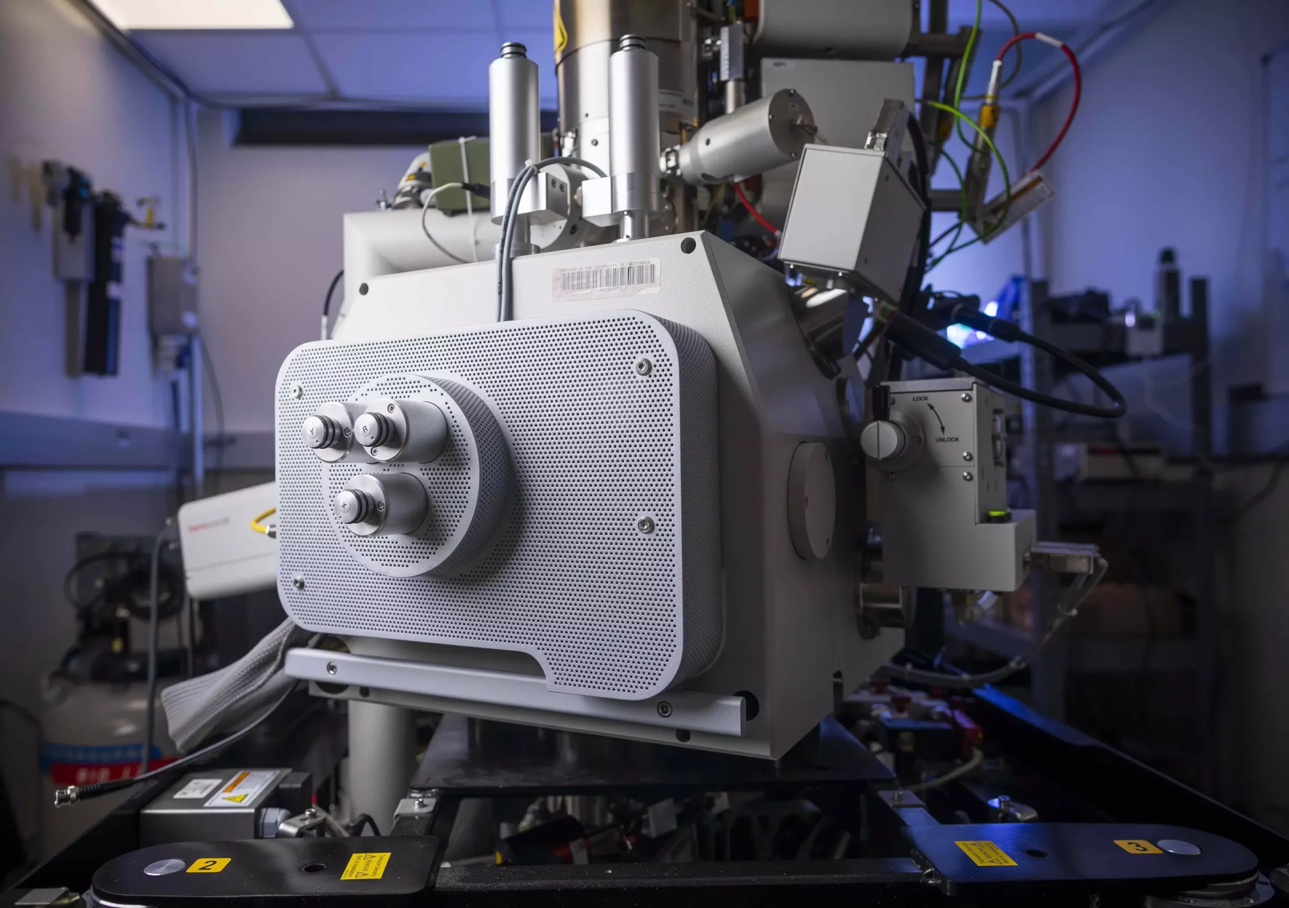
At the forefront of semiconductor research, a team from UC Santa Barbara has achieved a monumental breakthrough: the first-ever visualization of electric charges as they traverse the boundary of two different semiconductor materials. This exceptional feat, showcased through advanced scanning ultrafast electron microscopy (SUEM), shatters previous limitations in observing these rapid phenomena. Led by Bolin Liao, an associate professor of mechanical engineering, the findings, published in the Proceedings of the National Academy of Sciences, provide unprecedented insights into electric charge dynamics that were previously understood through indirect measurement.
Historically, semiconductor theory has been largely theoretical, supported by a plethora of texts that explore the behavior of electronic charges. Yet, for years, researchers have struggled to directly observe these fleeting processes. “There are many indirect measurements,” Liao commented, underlining the importance of direct observation in bolstering the semiconductor theory. This groundbreaking visualization allows material scientists to validate existing theoretical frameworks, enhancing our overall understanding of semiconductor physics.
The implications of this research extend well beyond academic interest. In practical terms, it has significant ramifications for the design and efficiency of devices that rely on semiconductor materials, particularly solar cells. In a standard photovoltaic system, when sunlight excites electrons, these “photocarriers” create a flow of electric current through their movement. However, a crucial limitation is that these electrons will lose energy in mere picoseconds, leading to inefficiencies as they transition to a cooler state, discarding an abundance of excess energy as waste heat.
The core of this research revolves around a pivotal area known as heterojunctions—the interfaces between two different semiconductor materials. These heterojunctions are central to a variety of applications, ranging from laser technology to sensor development. To unearth the characteristics of hot carriers at such junctions, Liao and his colleagues directed their SUEM apparatus at a specifically designed heterojunction of silicon and germanium—a combination praised for its potential in the technological arena.
Their innovative approach leverages ultrafast laser pulses to effectively capture snapshots of the photocarriers as they navigate through semiconductor materials. By employing a picosecond-scale shutter alongside an electron beam, they can illuminate events occurring within an incredibly brief timescale, ranging from picoseconds to nanoseconds. “The real excitement stems from our capacity to visualize how the charges transfer across the junction,” Liao elaborated, illuminating the importance of such visual evidence.
The images produced from this technique reveal profound interactions among photocarriers, showcasing their swift movement from one semiconductor to the other. Liao described the initial velocity of these hot carriers as impressively rapid, driven by their elevated temperature. However, as charges pass near the junction, a fraction becomes ensnared by the junction’s potential. This trapping phenomenon results in diminished mobility, ultimately hindering the performance of devices designed to segregate and harness these carriers.
These observations were particularly striking, as they provided direct experimental evidence supporting longstanding semiconductor theories. Liao expressed his surprise at being able to visualize this effect, highlighting its potential implications for semiconductor device designers who might need to find ways to mitigate such trapping effects. This newfound capability not only sheds light on existing problems but also poses questions for the future development of semiconductor technologies.
This remarkable study represents a significant chapter in the ongoing evolution of semiconductor technology, resonating deeply with the legacy of Herb Kroemer, the esteemed UCSB engineering professor who first postulated the concept of heterostructures in semiconductors back in 1957. His assertion that “the interface is the device” laid the groundwork for what would become the backbone of modern microelectronics and information systems.
The recent research marks a return to foundational ideas, providing a more complete understanding of electric charge behavior at the junctions of materials. By enhancing the visualization techniques in studying these phenomena, Liao’s team has opened a new avenue for innovators and researchers alike, reaffirming the importance of refining our comprehension of charge transport in the ever-evolving realm of semiconductor research. As the field moves forward, the insights gained from this study hold the promise of fostering advances in energy efficiency and device performance that could have lasting impacts on technology utilized in everyday life.


Leave a Reply