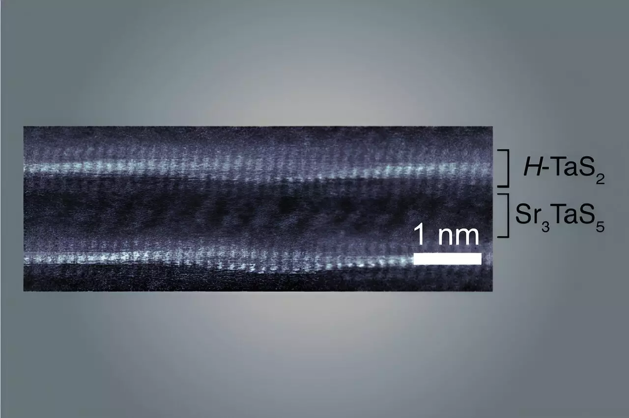
Recent advancements in material science have led to an exciting discovery by a team of researchers from MIT. They have engineered a new type of material that combines unique superconducting and metallic features, achieved through a fascinating arrangement of atomic layers that are each just a billionth of a meter thick. This innovative structure consists of repetitive wavy layers of atoms, creating a macroscopic sample that can be handled and studied in ways that were previously impossible with other materials of similar dimensional characteristics. The findings were published in the prestigious journal *Nature*, signaling a significant leap forward in our understanding of quantum behavior at the atomic level.
Unlike traditional materials that require extreme precision and manual assembly, this new class of material has been synthesized through what the team describes as rational design. This approach involves leveraging insights from both materials science and chemistry to formulate a “recipe” for creating these novel substances. Consequently, the researchers express optimism about the potential for developing additional materials with unconventional properties. The unique structural integrity of the material—consistently wavy atomic arrangements—differentiates it from existing materials with similar traits.
The fascination with two-dimensional materials, which consist of one or a few atomic layers, has become a focal point for physicists in recent years. The properties of these materials can be drastically altered simply by manipulating their orientation. For example, when layers are twisted at slight angles, they form a moiré superlattice—an intricate pattern that results in a broad spectrum of phenomena, including superconductivity and exotic magnetism. However, creating these moiré structures comes with its own challenges, as they require painstaking manual assembly and precise measurements.
To circumvent these obstacles, the researchers at MIT have developed methods to fabricate analogous materials that maintain the fascinating properties of two-dimensional structures while being easier to manipulate and study. By using powdered materials subjected to high-temperature conditions, they can naturally form large single crystals that exhibit behavior rooted in atomic-scale interactions—a breakthrough process that simplifies prior methodologies.
The newly established material comprises alternating layers of tantalum and sulfur, interspersed with spacer layers made of strontium. This layered architecture resembles a multi-layer cake, where uniformity and coherence across thousands of layers contribute to the resulting crystal’s lucidity. The researchers suggest that the formation of waves within the material is due to mismatched crystal lattice characteristics among the layers. This concept can be likened to two sheets of paper—the legal and regular sizes—where the legal paper’s dimensions necessitate a buckling upwards to overlap the underlying sheet.
This structural configuration is pivotal, as it introduces an innovative paradigm within the superconducting realm. When the material is cooled to a specific temperature, it exhibits superconductivity—where electrons traverse through it with zero resistive loss. Interestingly, the very characteristics of the waves lead to varying intensities of superconductivity across different regions of the material. This variability is not just a curiosity; it represents a new avenue to explore how structural design at the atomic level can elicit diverse electronic behaviors.
Implications and Future Prospects
The researchers believe that by directing electron flow along the substrates formed by these waves—like navigating a ball down a trough rather than over a hill—they provide a sort of “directionality” to electron motion. This modification leads to much greater ease in electron movement along the layered structure, redefining our understanding of metallic properties in these materials.
By paving the way for future research, this new family of materials holds tremendous promise across various applications—from quantum computing to advanced electronics. It provides a foundation on which other scientists can build, furthering exploration into materials that might have once been confined to theoretical speculation. “We’ve planted the flag and opened up an entirely new territory of materials,” says one of the team members. The unexpected results emerging from this research not only bolster scientific knowledge but also exemplify how interdisciplinary collaboration can yield innovative breakthroughs in technology.
The MIT physicists’ findings encapsulate an exciting intersection of science and engineering, offering a potent reminder of the boundless potential inherent in the intricate world of materials at the atomic scale. As researchers continue to explore these uncharted realms, who knows what remarkable phenomena and extraordinary applications lie ahead?


Leave a Reply